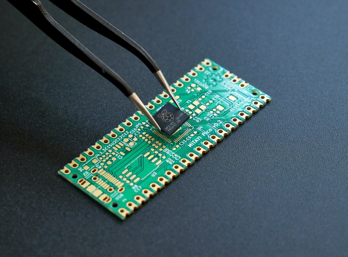
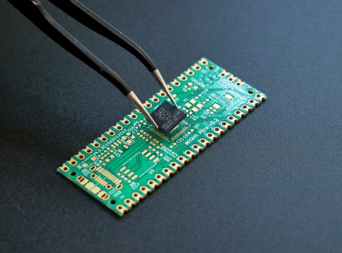
PCBA stands for Printed Circuit Board Assembly, which is the process of soldering electronic components onto a printed circuit board (PCB) to create a functioning electronic device. The process typically includes the following steps:

PCB Fabrication:
PCB (Printed Circuit Board) Fabrication is the process of creating the physical board that makes up the backbone of an electronic device. This process includes several steps including designing the circuit layout, creating a metal layer, drilling holes, adding metal layers, and applying a soldermask. The final product is then tested and inspected to ensure it meets the specifications.
The PCB fabrication process starts with creating a circuit design, typically done using computer-aided design (CAD) software. The design is then transferred onto a metal or plastic board using a process called photolithography. This involves applying a light-sensitive coating to the board and exposing it to light through a mask that corresponds to the circuit design. The board is then etched to remove any exposed metal and create the electrical pathways.
Next, holes are drilled into the board where electronic components will be soldered. The board is then coated with a metal layer, typically copper, to provide electrical connectivity. The final step is applying a soldermask, which is a protective coating that prevents unwanted electrical connections and helps to insulate the components.
Surface Mount Technology (SMT) Component Placement:
Surface Mount Technology (SMT) Component Placement is a process in PCB Manufacturing where tiny components are placed directly onto the surface of a printed circuit board (PCB) and soldered in place. This process is in contrast to through-hole technology, where components are inserted into holes in the PCB and soldered on both sides.
SMT component placement is done using a pick-and-place machine, which is a highly automated machine that can place components with high accuracy and speed. The machine uses a vacuum or a gripper to pick up components from a supply reel and place them onto the PCB. The components are then reflowed using heat to melt the solder and create a permanent bond with the PCB.
SMT component placement has several advantages over through-hole technology, including higher assembly speed, smaller board size, lighter weight, and improved reliability. Additionally, SMT components have smaller sizes and higher input/output count, making them ideal for use in modern electronics such as smartphones, laptops, and other portable devices.
Reflow Soldering:
Reflow soldering is a process in electronics manufacturing where soldering paste is used to join electronic components to a printed circuit board (PCB). Reflow soldering is used for Surface Mount Technology (SMT) components and is a critical step in the PCB manufacturing process.
The process of reflow soldering starts with applying a thin layer of soldering paste to the pads on the PCB where the components will be placed. The components are then placed onto the PCB using a pick-and-place machine. The assembled board is then placed into a reflow oven where the temperature is raised to a specific profile. The soldering paste melts and flows to form a permanent bond between the components and the PCB.
Reflow soldering has several advantages over traditional soldering methods, including improved consistency and reliability, higher assembly speed, and reduced manual labor. The process is also more environmentally friendly as it reduces the need for manual soldering and associated toxic fumes.
Through-hole Component Insertion:
Through-hole component insertion is a process in electronics manufacturing where components are inserted into holes drilled into a printed circuit board (PCB) and then soldered in place. This process is used for larger and more robust components and is a traditional method for attaching components to a PCB.
The process of through-hole component insertion starts with drilling holes into the PCB where the components will be inserted. The components are then inserted into the holes and the leads are bent to hold the components in place. The components are then soldered on both sides of the PCB to form a permanent electrical and mechanical connection.
Through-hole component insertion has several advantages over Surface Mount Technology (SMT) component placement, including higher reliability and improved mechanical strength. The process is also easier to repair if a component fails, as the components can be removed and replaced without damaging the PCB.
Inspection and Testing:
PCB (Printed Circuit Board) assembly inspection and testing are crucial steps in the manufacturing process to ensure that the final product meets the specifications and standards required. The inspection process may include visual inspection, X-ray inspection, AOI (Automated Optical Inspection), and functional testing. The testing process involves checking the electrical and functional aspects of the circuit board, including continuity testing, insulation resistance testing, and in-circuit testing. The purpose of these inspections and tests is to identify any defects or issues early in the manufacturing process, allowing for correction and improvement of the final product.
Check Also: 5 Tools For Electronic Repair For Beginners
Cleaning:
Cleaning is an important step in the process of circuit board component identification. This helps to remove any dirt, residue, or other contaminants that may affect the accuracy of the identification process. Cleaning can be done manually using a solvent such as isopropyl alcohol or ultrasonic cleaning, or it can be done automatically using specialized cleaning equipment. The type of cleaning method used depends on the complexity of the circuit board and the type of components being identified. Cleaning ensures that the surface of the circuit board and components are free from any contaminants, which can improve the accuracy of the component identification process and ultimately result in a better functioning circuit board.
Packaging and Shipping:
Packaging and shipping of printed circuit board (PCB) connectors is an important step in the manufacturing process to ensure the safe and secure delivery of the product to the customer. Proper packaging protects the PCB connectors from physical damage during transportation and storage and helps to maintain the integrity of the product.
There are various types of packaging materials used for PCB connectors, including anti-static bags, bubble wrap, foam, and ESD (ElectroStatic Discharge) protective packaging. The selection of the packaging material depends on the type of connector and the requirements of the customer.
In addition to packaging, labeling is also important for the identification and traceability of the PCB connectors during transportation and storage. The labels should include information such as the type of connector, the manufacturer, and the date of manufacture.
Finally, the packaged PCB connectors should be shipped using a reliable shipping method that provides adequate protection and meets the customer’s requirements. This may include air, sea, or ground transportation, and the choice of shipping method should take into account factors such as cost, delivery time, and product requirements.
The PCBA (Printed Circuit Board Assembly) manufacturing process is a complex and multi-step procedure that involves several stages, from design and prototyping to assembly and testing. The process involves the production of the circuit board, the placement of components, and the connection of those components to form a functioning electronic device.
Each stage of the PCBA manufacturing process is crucial to the final product and must be completed with precision and accuracy to ensure that the product meets the required specifications and standards. The process includes steps such as schematic design, PCB layout, drilling and etching, component placement, soldering, inspection, and testing.
Conclusion:
The PCBA manufacturing process is an essential part of the electronics industry and requires a combination of technical expertise and attention to detail to ensure that the final product meets the required standards and specifications. The process requires the use of specialized equipment and a team of skilled technicians to ensure that each stage of the process is completed correctly. The end result of the PCBA manufacturing process is a functional and high-quality electronic device that meets the needs of the customer.
Author
Tanvir Sakline, a local SEO expert, has been helping small businesses improve their online visibility and reach new customers through effective local citation-building and guest posting strategies. With a passion for digital marketing, Tanvir Sakline stays up-to-date with the latest industry trends and shares actionable insights. In their free time, Tanvir Sakline enjoys exploring new local restaurants and cafes and practicing photography.


